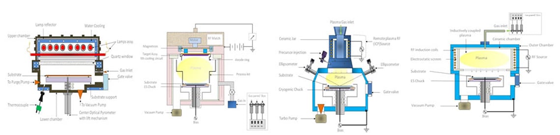
ASM has over 2000+ Person years of experience in serving reputed Semiconductor ‘Front-End’ and ‘Back-End’ process equipment manufacturing companies. ASM has the expertise and understanding of design & development of System and Sub Systems of: PVD, CVD, RTP, Etch, CMP and related Inspection/ process tools for Wafer Metallization and Packaging.
ASM’s Engineering Services across Customer’s spectrum of tools:
Design and Development from concept to realization
Continuous Improvement projects and Co-Creation
Application Software Development and Support
Industrial IoT
Virtual Reality (VR)
Sustenance Engineering
Operations support
24/7 Infrastructure/ Network Management and support